 +91 7483031199
- 0820-2589182
- info@sode-edu.in
- CET CODE-E206
- Career Opportunities
 The main objective of the industry visit was to bridge the gap between theoretical knowledge and practical exposure by providing students with insights into the semiconductor design and development process. The visit aimed to enhance students’ understanding of VLSI design, semiconductor technologies, layout design practices, and industry requirements, while also encouraging them to explore emerging opportunities in the electronics sector.
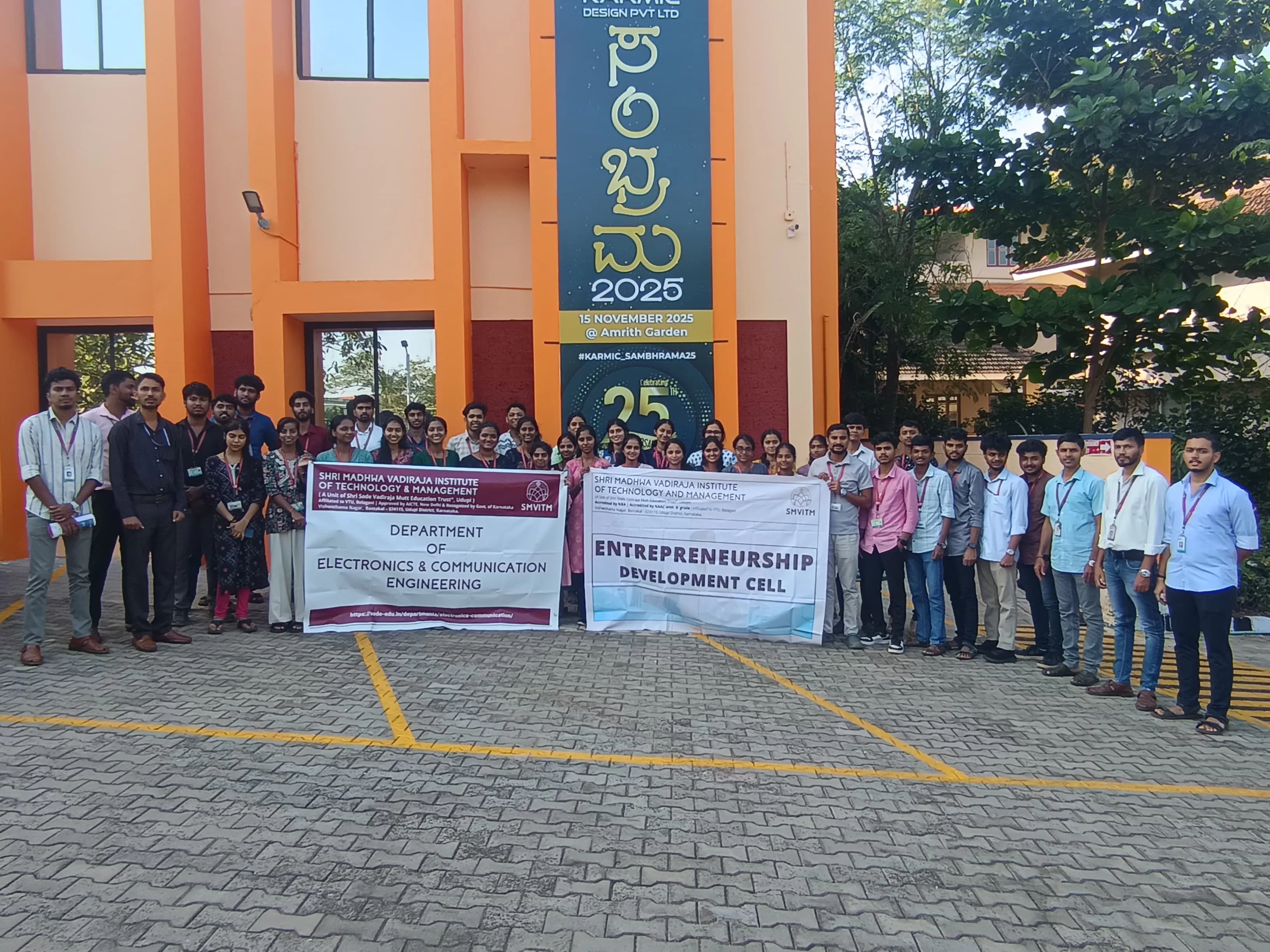
Brief Report of the Activity
The visit began with an overview of KARMIC Design Pvt. Ltd., highlighting the company’s expertise in semiconductor design and its contributions to the global electronics industry. Students were introduced to different types of semiconductor industries and their applications. The session also focused on the core values and competencies required for engineers in this field, such as innovation, precision, teamwork, and continuous learning.
The technical sessions provided detailed exposure to several important VLSI concepts, including:
Introduction to VLSI and its role in modern electronics
PMOS, NMOS, CMOS, and FinFET cross-sections, fabrication processes, and performance characteristics
Building blocks of LDO (Low Dropout Regulator), including schematic design, layout floorplan, and working principles
Input pair and current mirrors, highlighting the importance of matching in analog circuits
I/O pads, including floorplan and schematic design considerations
Different types of chip packaging and their relevance in semiconductor manufacturing
Complete VLSI design flow, from specification to fabrication
Throughout the visit, students actively interacted with the resource persons, who shared valuable professional insights and guided students on aligning academic learning with industry expectations. The importance of design accuracy, teamwork, and continuous skill enhancement in the semiconductor domain was also emphasized.